- 您现在的位置:买卖IC网 > Sheet目录3886 > PIC16LCE624-04E/SO (Microchip Technology)IC MCU CMOS 1K OTP W/EEPRM18SOIC
1999 Microchip Technology Inc.
DS40182C-page 39
PIC16CE62X
7.3.1
SWITCHING PRESCALER ASSIGNMENT
The prescaler assignment is fully under software
control (i.e., it can be changed “on-the-fly” during
program execution). To avoid an unintended device
RESET,
the
following
instruction
sequence
(Example 7-1) must be executed when changing the
prescaler assignment from Timer0 to WDT.
EXAMPLE 7-1:
CHANGING PRESCALER
(TIMER0
→WDT)
1.BCF
STATUS, RP0
;Skip if already in
; Bank 0
2.CLRWDT
;Clear WDT
3.CLRF
TMR0
;Clear TMR0 & Prescaler
4.BSF
STATUS, RP0
;Bank 1
5.MOVLW
'00101111’b
;These 3 lines (5, 6, 7)
6.MOVWF
OPTION
; are required only if
; desired PS<2:0> are
7.CLRWDT
; 000 or 001
8.MOVLW
'00101xxx’b
;Set Postscaler to
9.MOVWF
OPTION
; desired WDT rate
10.BCF
STATUS, RP0
;Return to Bank 0
To change prescaler from the WDT to the TMR0
module, use the sequence shown in Example 7-2. This
precaution must be taken even if the WDT is disabled.
EXAMPLE 7-2:
CHANGING PRESCALER
(WDT
→TIMER0)
CLRWDT
;Clear WDT and
;prescaler
BSF
STATUS, RP0
MOVLW
b'xxxx0xxx'
;Select TMR0, new
;prescale value and
;clock source
MOVWF
OPTION_REG
BCF
STATUS, RP0
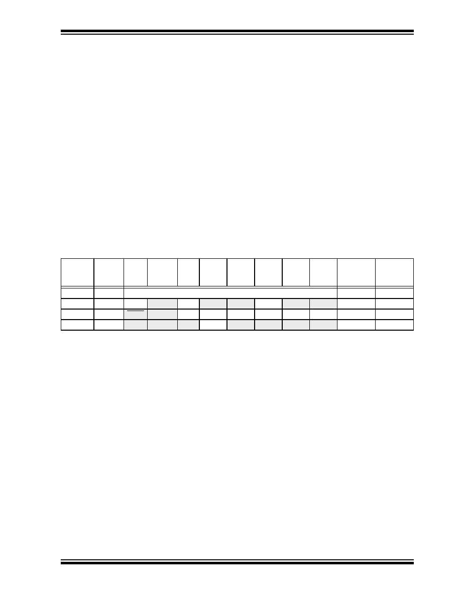
TABLE 7-1:
REGISTERS ASSOCIATED WITH TIMER0
Address
Name
Bit 7
Bit 6
Bit 5
Bit 4
Bit 3
Bit 2
Bit 1
Bit 0
Value on:
POR
Value on
All Other
Resets
01h
TMR0
Timer0 module register
xxxx xxxx
uuuu uuuu
0Bh/8Bh
INTCON
GIE
PEIE
T0IE
INTE
RBIE
T0IF
INTF
RBIF
0000 000x
0000 000u
81h
OPTION
RBPU
INTEDG
T0CS
T0SE
PSA
PS2
PS1
PS0
1111 1111
85h
TRISA
—
—TRISA4
TRISA3
TRISA2
TRISA1
TRISA0
---1 1111
Legend: — = Unimplemented locations, read as ‘0’, x = unknown, u = unchanged.
Note:
Shaded bits are not used by TMR0 module.
发布紧急采购,3分钟左右您将得到回复。
相关PDF资料
PIC16F1829-I/SO
MCU PIC 14K FLASH 1K RAM 20SOIC
PIC16F685-I/SS
IC PIC MCU FLASH 4KX14 20SSOP
PIC16LCE624-04E/P
IC MCU CMOS 1K OTP W/EEPRM 18DIP
PIC16F689-I/SS
IC PIC MCU FLASH 4KX14 20SSOP
PIC16C54C-04I/SO
IC MCU OTP 512X12 18SOIC
PIC16C54C-04/SO
IC MCU OTP 512X12 18SOIC
PIC16F722-I/ML
IC PIC MCU FLASH 2KX14 28-QFN
PIC16LCE623T-04I/SO
IC MCU CMOS.5K OTP W/EEPRM18SOIC
相关代理商/技术参数
PIC16LCE624-04E/SS
功能描述:8位微控制器 -MCU 1.75KB 96 RAM 13 I/O RoHS:否 制造商:Silicon Labs 核心:8051 处理器系列:C8051F39x 数据总线宽度:8 bit 最大时钟频率:50 MHz 程序存储器大小:16 KB 数据 RAM 大小:1 KB 片上 ADC:Yes 工作电源电压:1.8 V to 3.6 V 工作温度范围:- 40 C to + 105 C 封装 / 箱体:QFN-20 安装风格:SMD/SMT
PIC16LCE624-04I/P
功能描述:8位微控制器 -MCU 1.75KB 96 RAM 13 I/O RoHS:否 制造商:Silicon Labs 核心:8051 处理器系列:C8051F39x 数据总线宽度:8 bit 最大时钟频率:50 MHz 程序存储器大小:16 KB 数据 RAM 大小:1 KB 片上 ADC:Yes 工作电源电压:1.8 V to 3.6 V 工作温度范围:- 40 C to + 105 C 封装 / 箱体:QFN-20 安装风格:SMD/SMT
PIC16LCE624-04I/SO
功能描述:8位微控制器 -MCU 1.75KB 96 RAM 13 I/O RoHS:否 制造商:Silicon Labs 核心:8051 处理器系列:C8051F39x 数据总线宽度:8 bit 最大时钟频率:50 MHz 程序存储器大小:16 KB 数据 RAM 大小:1 KB 片上 ADC:Yes 工作电源电压:1.8 V to 3.6 V 工作温度范围:- 40 C to + 105 C 封装 / 箱体:QFN-20 安装风格:SMD/SMT
PIC16LCE624-04I/SS
功能描述:8位微控制器 -MCU 1.75KB 96 RAM 13 I/O RoHS:否 制造商:Silicon Labs 核心:8051 处理器系列:C8051F39x 数据总线宽度:8 bit 最大时钟频率:50 MHz 程序存储器大小:16 KB 数据 RAM 大小:1 KB 片上 ADC:Yes 工作电源电压:1.8 V to 3.6 V 工作温度范围:- 40 C to + 105 C 封装 / 箱体:QFN-20 安装风格:SMD/SMT
PIC16LCE624T-04/SO
功能描述:8位微控制器 -MCU 1.75KB 96 RAM 13 I/O RoHS:否 制造商:Silicon Labs 核心:8051 处理器系列:C8051F39x 数据总线宽度:8 bit 最大时钟频率:50 MHz 程序存储器大小:16 KB 数据 RAM 大小:1 KB 片上 ADC:Yes 工作电源电压:1.8 V to 3.6 V 工作温度范围:- 40 C to + 105 C 封装 / 箱体:QFN-20 安装风格:SMD/SMT
PIC16LCE624T-04/SS
功能描述:8位微控制器 -MCU 1.75KB 96 RAM 13 I/O RoHS:否 制造商:Silicon Labs 核心:8051 处理器系列:C8051F39x 数据总线宽度:8 bit 最大时钟频率:50 MHz 程序存储器大小:16 KB 数据 RAM 大小:1 KB 片上 ADC:Yes 工作电源电压:1.8 V to 3.6 V 工作温度范围:- 40 C to + 105 C 封装 / 箱体:QFN-20 安装风格:SMD/SMT
PIC16LCE624T-04E/SO
功能描述:8位微控制器 -MCU 1.75KB 96 RAM 13 I/O RoHS:否 制造商:Silicon Labs 核心:8051 处理器系列:C8051F39x 数据总线宽度:8 bit 最大时钟频率:50 MHz 程序存储器大小:16 KB 数据 RAM 大小:1 KB 片上 ADC:Yes 工作电源电压:1.8 V to 3.6 V 工作温度范围:- 40 C to + 105 C 封装 / 箱体:QFN-20 安装风格:SMD/SMT
PIC16LCE624T-04E/SS
功能描述:8位微控制器 -MCU 1.75KB 96 RAM 13 I/O RoHS:否 制造商:Silicon Labs 核心:8051 处理器系列:C8051F39x 数据总线宽度:8 bit 最大时钟频率:50 MHz 程序存储器大小:16 KB 数据 RAM 大小:1 KB 片上 ADC:Yes 工作电源电压:1.8 V to 3.6 V 工作温度范围:- 40 C to + 105 C 封装 / 箱体:QFN-20 安装风格:SMD/SMT